
In memory of Terry Gillett
Terry Gillett passed away last Saturday after a three year battle with cancer. If you have been involved in any way with Village Telco, you… Read More »In memory of Terry Gillett
Terry Gillett passed away last Saturday after a three year battle with cancer. If you have been involved in any way with Village Telco, you… Read More »In memory of Terry Gillett

Digital Library The Digital Library Project provides a simple way to serve a wide variety of essentially static web content in a classroom situation where… Read More »Learning Platform Project
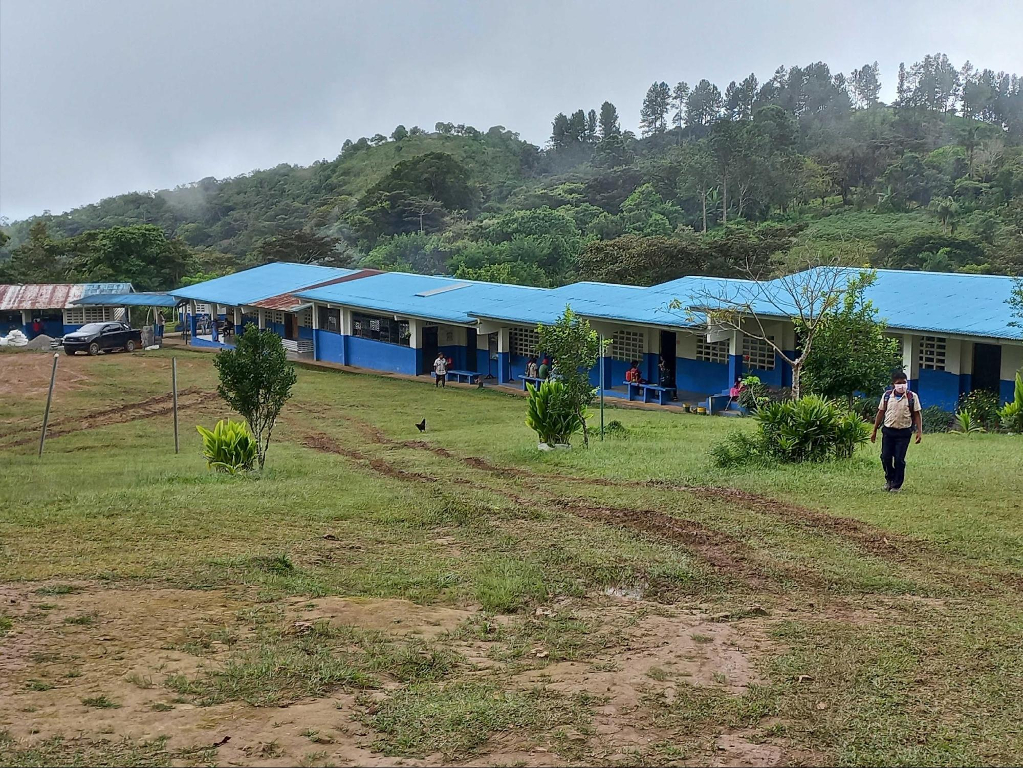
Digital Libraries have been deployed in a number of locations including Panama, Pakistan, Cambodia and Timor Leste. Brief descriptions of these deployments can be found… Read More »Digital Library Deployment Projects