
In electronic hardware design you can be sure that anything new and untested will have bugs. So I have a habit of building the new part and testing it using known working hardware. The engineering concept is to test and debug the absolute minimum, as bug counts tend to increase exponentially with complexity.
With the Mesh Potato the FXS Interface hardware is new. This design connects the router to an analog telephone. So Elektra and I have designed a small PCB to test just that part of the design. Here are some pictures of (i) the small FXS interface PCB design we have designed and (ii) an assembled FXS interface PCB, with a WRT54 for scale.
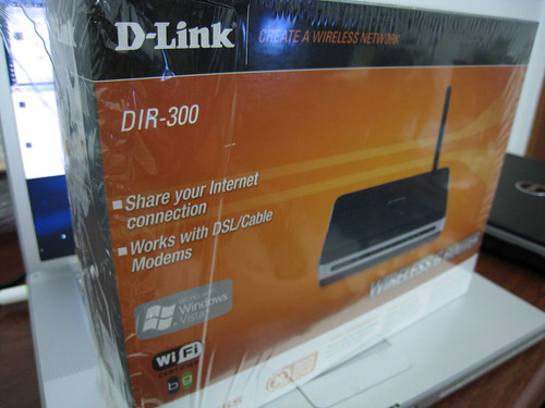
The idea is to connect this PCB to a Nanostation 2 or DIR-300 router and build up the Mesh Potato FXS functionality. We can then incorporate any bug fixes into the Mesh Potato prototype.
This strategy is also a time saver – while Atcom are laying out and building the PCB for the Mesh Potato Prototype, we can be using the FXS interface hardware above to develop the Mesh Potato software. That way we reduce the overall length of the project as when the Mesh Potato Prototype arrives we will have tested and debugged firmware to run on it.
We have plenty of spare PCBs so if any one would like to build up a FXS interface please let me know.
